|
!WARNING
· Use PPTC beyond the maximum ratings or improper use may result in device damage and possible electrical arcing and flame.
· PPTC are intended for protection against occasional over current or over temperature fault conditions and should not be used when repeated
fault conditions or prolonged trip events are anticipated.
· Device performance can be impacted negatively if devices are handled in a manner inconsistent with recommended electronic, thermal, and
mechanical procedures for electronic components.
· Use PPTC with a large inductance in circuit will generate a circuit voltage (L di/dt) above the rated voltage of the PPTC.
· Avoid impact PPTC device its thermal expansion like placed under pressure or installed in limited space.
· Contamination of the PPTC material with certain silicon based oils or some aggressive solvents can adversely impact the performance of the
devices. PPTC SMD can be cleaned by standard methods.
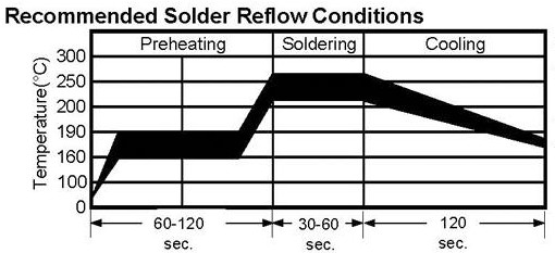
· Requests that customers comply with our recommended solder pad layouts and recommended reflow profile. Improper board layouts or
reflow profile could negatively impact solderability performance of our devices.
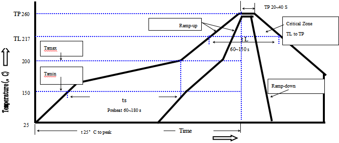
Soldering Parameters

|
Profile Feature
|
Pb-Free Assembly
|
|
Average Ramp-Up Rate(Ts max to T p)
|
3℃/second mac.
|
|
Preheat
-Temperature Min(Ts min)
-Temperature Max(Ts max)
-Time(Ts min to Ts max)
|
150℃
200℃
60~180 seconds
|
|
Time maintained above:
-Temperature(TL)
-Time(tL)
|
217℃
60~150 seconds
|
|
Peak Temperature(Tp)
|
260℃
|
|
Ramp-Down Rate
|
6℃/second max.
|
|
Time 25℃ to Peak Temperature
|
8 minutes max
|
|
Storage Condition
|
0℃~30℃,30%-60%RH
|
Recommended reflow methods: IR, vapor phase oven, hot air oven, N2 environment for lead-free
Recommended maximum paste thickness is 0.25mm
Devices can be cleaned using standard industry methods and solvents.
Note 1:All temperature refer to topside of the package, measured on the package body surface.
Note 2: If reflow temperatures exceed the recommended profile, devices may not meet the performance requirements.
|


